0571-26692003
No. 181 Geyazhuang, Xihu District,Hangzhou, Zhejiang, P.R. China


The project has overcome the technical challenges of mass-producing 6-inch diamond wafers. By exploring diamond's potential as the "ultimate semiconductor", it advances disruptive applications and the industrialization of power electronic devices and novel lasers based on single-crystal diamond.
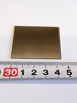
1. Industrial-grade single-crystal diamond wafers
Achieved breakthroughs in the growth and mass production technology for wafers exceeding 2 inches, enabling batch production of industrial-grade diamond.
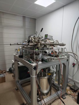
2. Large-wafer MPCVD equipment
Developed internationally advanced MPCVD equipment for 6-inch wafers, with future potential to support 8-inch capability.
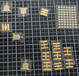
3. Development of market application use cases for diamond
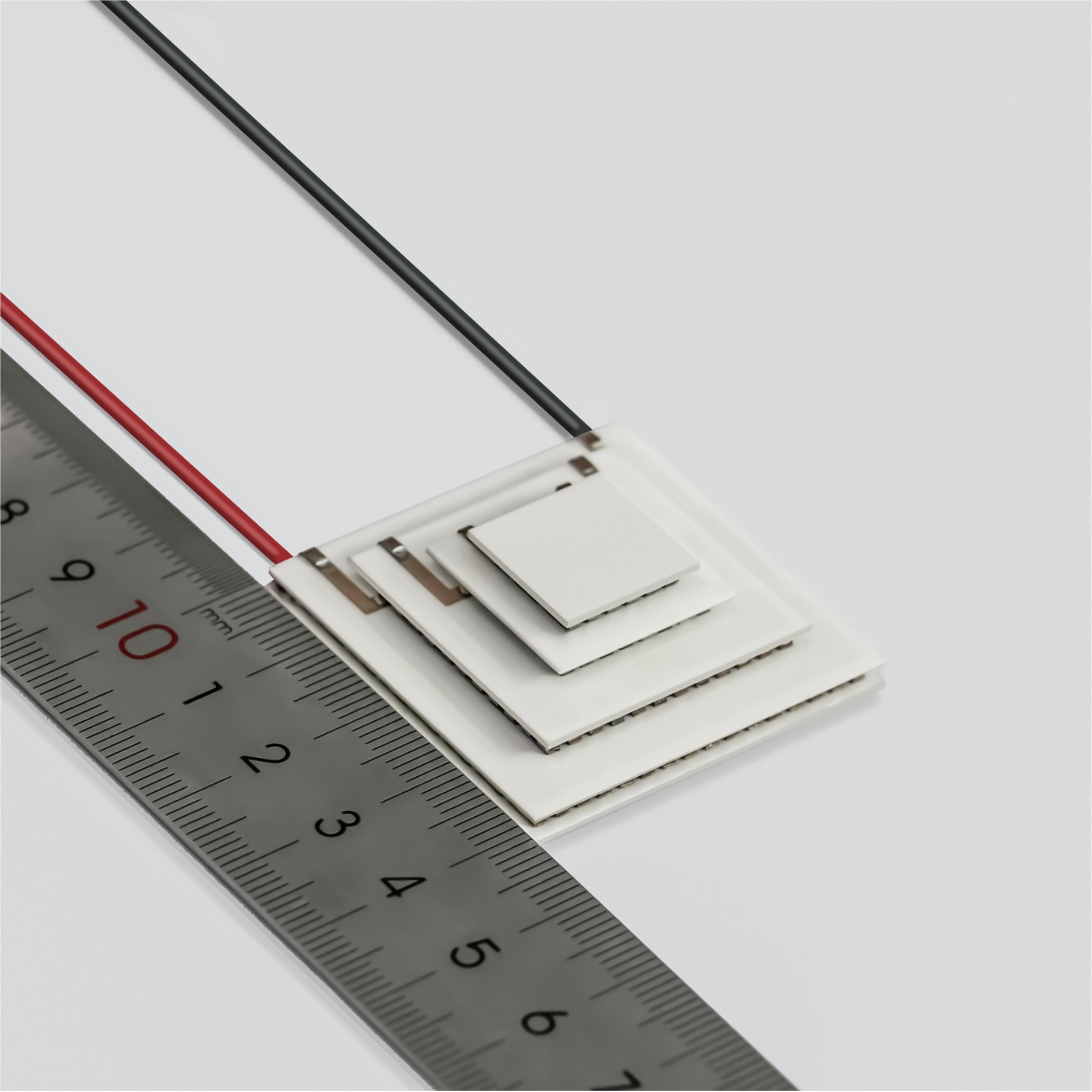
Explored application fields for materials and devices, including high-quality lab-grown diamonds, terahertz optical windows, high-energy detectors, and Schottky Barrier Diode (SBD) power devices.
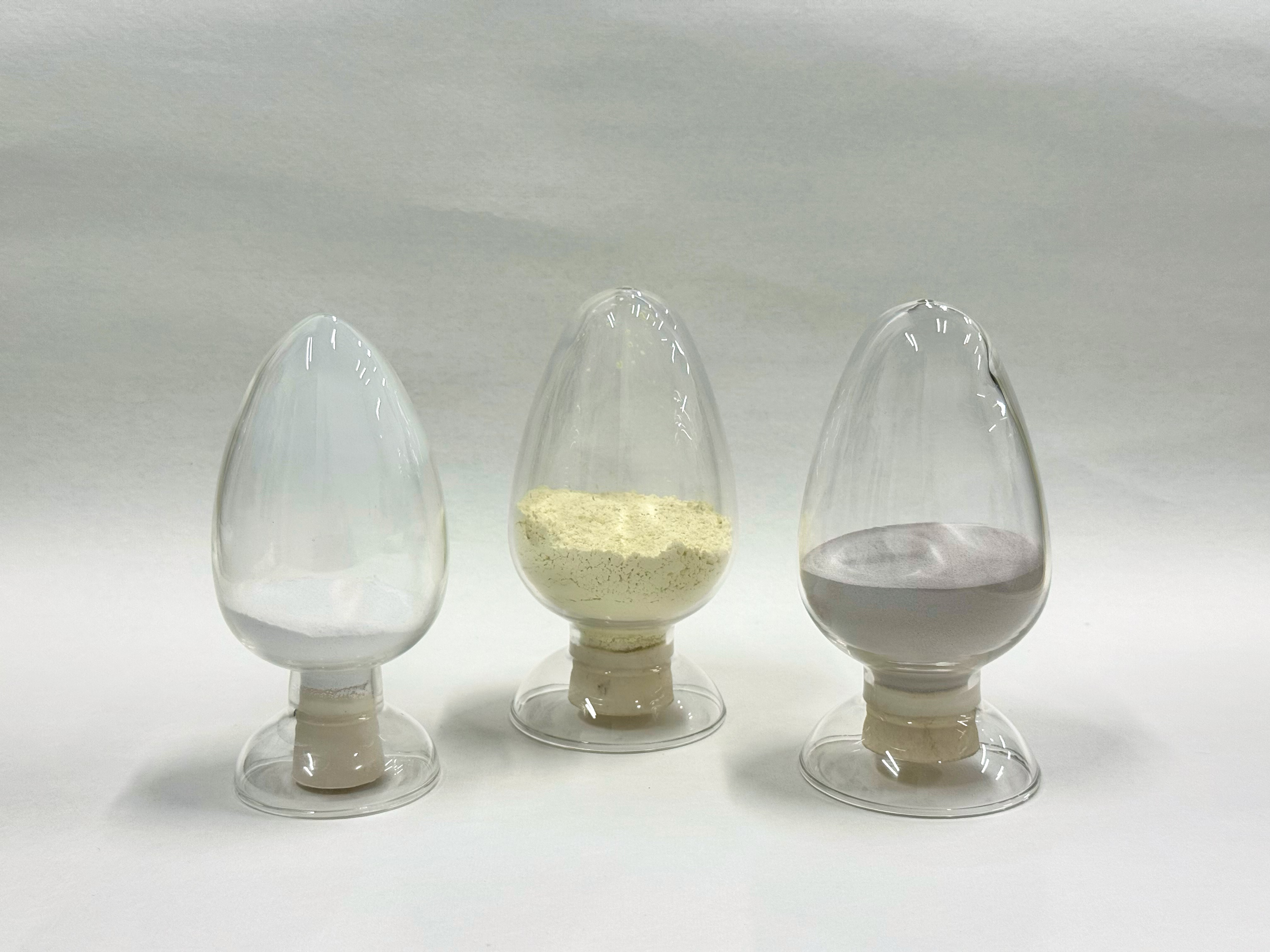
1. Lab-grown diamonds
Based on high-quality large single-crystal diamond growth technology, achieved product upgrades in lab-grown diamonds in the jewelry industry.
2. Wafer-related products
Utilizing 6-inch wafer growth technology, it can be applied to polycrystalline diamond heat sinks, high-quality semiconductor film substrates, optical windows, precision cutting tools, and other fields.