0571-26692003
No. 181 Geyazhuang, Xihu District,Hangzhou, Zhejiang, P.R. China
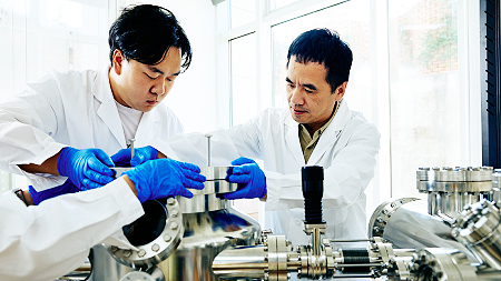
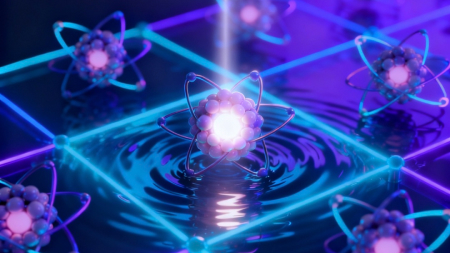
The Laboratory of Atomic-Scale Physics and Devices aims to advance cutting-edge scanning tunneling microscopy (STM) technology and develop novel semiconductor materials and practical devices. By integrating strong magnetic field technology and ultrafast spectroscopy techniques with STM, we seek to push the experimental boundaries of spatial, temporal, and energy resolution to explore novel phenomena in quantum materials. We also focus on the potential of diamond as the "ultimate semiconductor", advancing disruptive applications and industrialization of single-crystal diamond-based power electronic devices and next-generation laser systems.
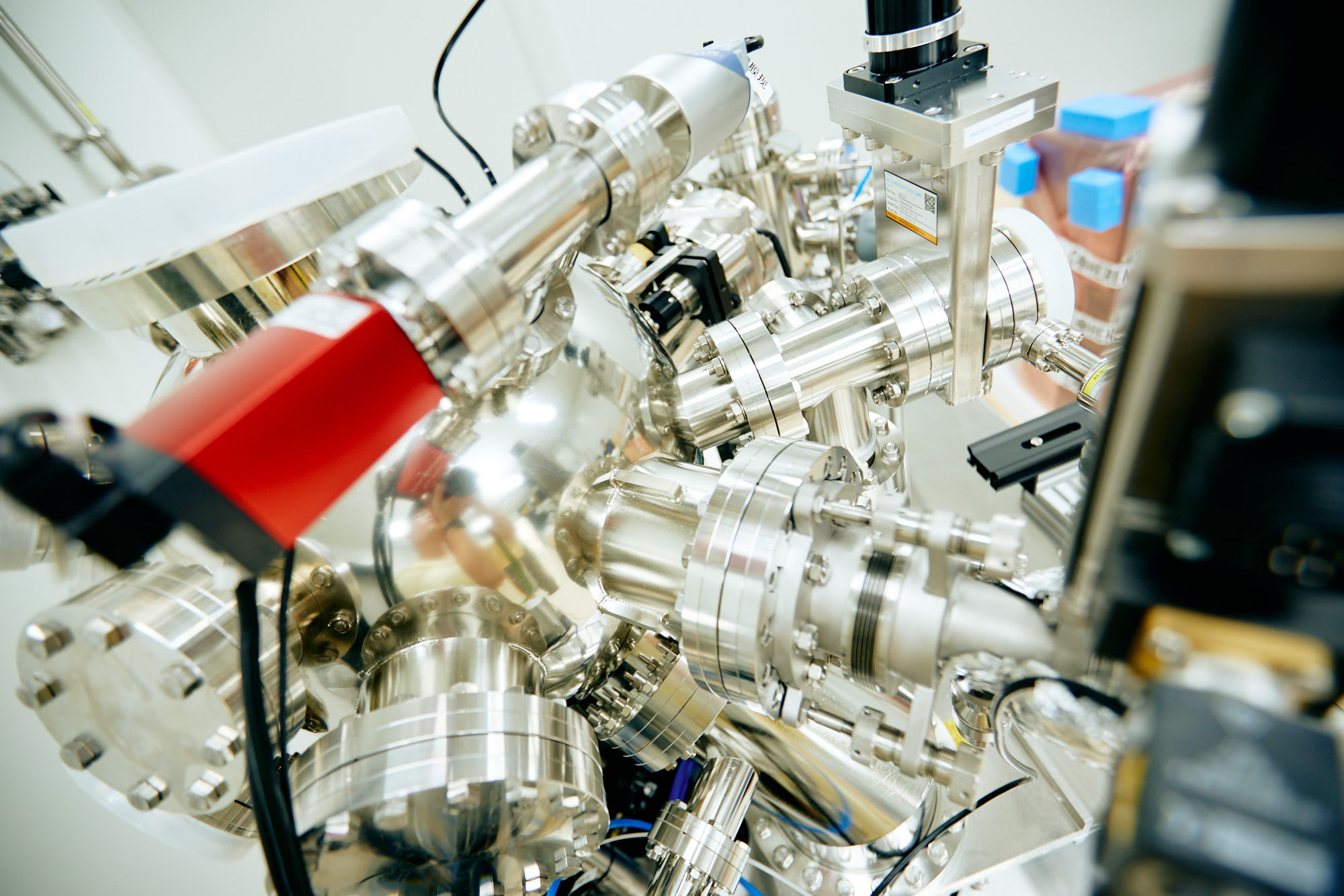
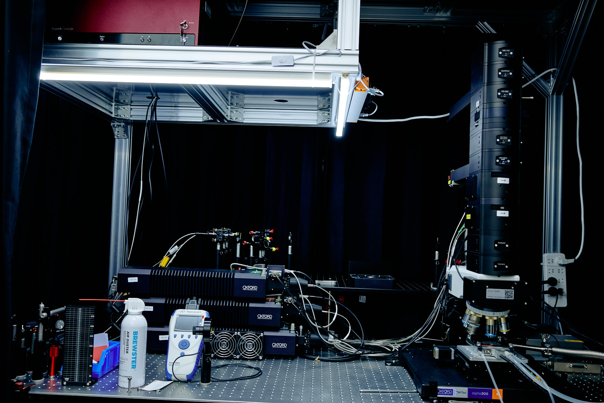
1. Development of advanced STM systems: including closed-cycle, helium-free cryogenic (300 mK) high-magnetic-field (9 T) STM, ultrafast femtosecond STM, and terahertz STM.
2. Design, fabrication, and characterization of low-dimensional quantum materials, focusing on the synthesis and investigation of novel functional oxide systems, two-dimensional ferroelectric, ferromagnetic, topological materials as well as the construction of their heterostructures, and the control of quantum phenomena through multi-field coupling and advanced nonlinear spectroscopic techniques;
3. Development and application of diamond materials and devices, focusing on the synthesis of large-size single-crystal diamond wafers and their application in optoelectronic functional devices.